
Low Voltage Electron Microscopes (LVEM)

Asia Mattelab is the distributor for Delong Instruments complete range of Low Voltage Electron Microscopes for Life Sciences and Materials Sciences applications. Delong Instruments Company is based in Brno, Czech Republic – the world capital of electron microscopy. Delong Instruments has more than 25 years of experience in the field of transmission electron microscopy (TEM). The company is also developing advanced electron-optical instruments, providing engineering design services and manufacturing precision parts and vacuum technology. Its main objective is to make electron microscopes more accessible and practical. That is why Delong Instruments puts extra emphasis on keeping microscopes innovative, compact, and easy to install, maintain and operate. Delong Instruments has developed the world’s first table-top TEM and specializes in low electron energy, which helps their microscopes to achieve high contrast of light elements and low radiation load, thus extending the range of observation methods. (See Delong Instruments)
The long-term and important partnership between Delong Instruments and Delong America have allowed the Delong Group to excel in operations in the high tech, engineering design, manufacturing and sales sectors. The Delong Group now spans 2 continents with operations in both Europe and North America. (See Delong)
Learn about the history of the development behind the low voltage electron microscope
Low Voltage Electron Microscope LVEM5
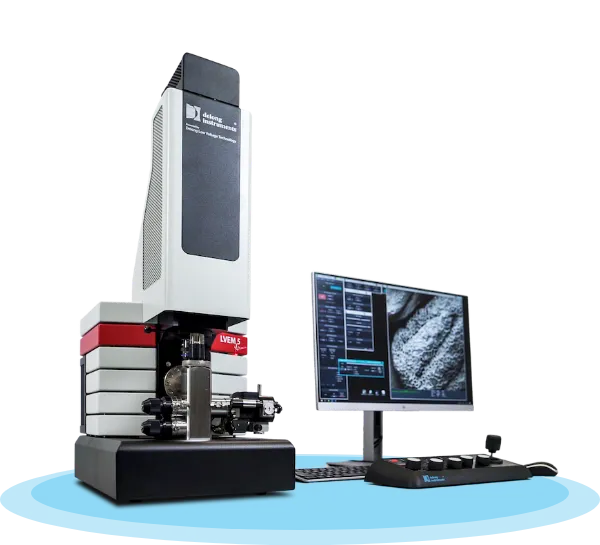
The LVEM 5 is the uniquely designed benchtop low voltage electron microscope that is small enough to fit anywhere nanoscale imaging is needed. A remarkable imaging tool equipped with TEM, SEM and STEM modes and designed to produce detailed and meaningful image results with unmatched contrast of biologic and soft material samples. The LVEM 5 is a benefit to any lab working, researching or studying nanomaterials.
The LVEM 5 is easy to learn, operate and maintain, and has a price that is just a fraction of the cost of a conventional transmission electron microscope. It is a versatile and capable instrument well-suited for any classroom or research lab. The LVEM 5 brings nanoscale to your benchtop.
LVEM5
Compact Low Voltage Electron Microscope LVEM25
All in One EM
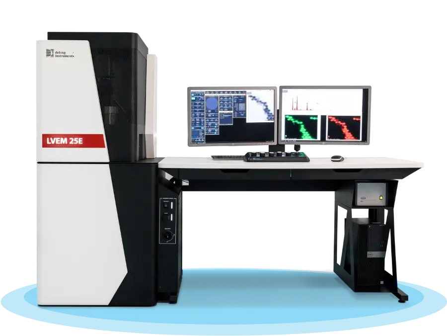
Equipped with five imaging and analysis modes, the LVEM 25E takes research to the next level. Its super-fast sample exchange and enhanced automation make it a practical, easy-to-use tool for routine imaging applications. The LVEM 25E delivers high-contrast, detailed images from samples prepared with standard protocols and offers the option to achieve the same level of detail with reduced staining.
Beyond imaging, the LVEM 25E enables comprehensive analysis of both internal and external structures, as well as the chemical composition of samples— all within a single device. Advanced software automatically sets column alignments and aperture positions, streamlining the user experience.
Fully integrated and portable design
- Extremely compact, space-saving, and portable design
- Single-plug installation in nearly any laboratory environment
- No special facility requirements (no cooling, power or anti-vibration isolation needed)
High contrast and resolution for standard samples
- Unmatched contrast of biologic and light material samples
- Achieve meaningful results with reduced staining
- Image resolution as good as 1.0 nm
- Designed for conventionally prepared samples
- Super-fast sample exchange
Five imaging modes in one instrument
- Equipped with TEM, STEM, SEM, EDS and ED modes
- Easily switch between imaging modes via intuitive software
- Bright and dark field measurements in both TEM and STEM modes
- SEM mode (BSE) for surface measurements
- Energy Dispersive Spectroscopy (EDS) for elemental analysis
- Electron Diffraction (ED) for understanding crystal structure
Imaging Modes
| TEM | ||
| Nominal accelerating voltage | 25 kV | |
| Resolution | 1.0 nm | |
| Total magnification | Display 3,800 – 3,000,000× Sensor 160-64,000x | |
| Magnification in Low mag regime | Display* 1,300× Sensor 54x | |
| Field of view | 100 – 0.25 μm | |
| Field of view in Low mag regime | 225 μm | |
| *valid for image on display at binning 2×2 | ||
| ELECTRON DIFFRACTION | ||
| Probe size | 500 – 8,000 nm | |
| Camera length (binning 2×2) | 2,000 – 5,000 pixels | |
| Camera constant (binning 2×2) | 17 – 40 nm pixels | |
| STEM | STEM 10 | STEM 15 |
| Nominal accelerating voltage | 10 kV | 15 kV |
| Resolving power | 1.0 nm | 1.0 nm |
| Magnification | 1,150-3,600,000× | 1,300-4,600,000x |
| Maximum field of view | 81 μm | 56 μm |
| SEM (BSE DETECTOR) | SEM 15 | |
| Nominal accelerating voltage | 15 kV | |
| Resolving power | 2 nm | |
| Magnification | 1,300-4,600,000x | |
| Maximum field of view | 105 μm | |
| EDS | ||
| Detector type | Silicon Drift Detector (SDD) | |
| Detector active area | 30 mm2 | |
| X-Ray Window | Windowless | |
| Energy Resolution | Mn Kα ≤ 129 eV | |
| Maximum throughput | 130 000 cps | |
| Hardware integration | Fully embedded | |
| Software | Esprit 2.3 | |
| STEM IMAGE CAPTURE | |
| up to 2,048 × 2,048 pxls/8 bits | |
| TEM IMAGE CAPTURE | |
| Camera | sCMOS |
| Sensor size | 2,048 × 2,048 pixels |
| Digitalization | 16-bits |
| SEM IMAGE CAPTURE | |
| Up to 2,048 × 2,048 pxls/8 bits | |